Discover the "Cleanroom" for teaching and research at UC Chile
The University is the first in South America to have this infrastructure, which is key for research. The room gives students access to state-of-the-art technology and equipment for micro and nanofabrication.
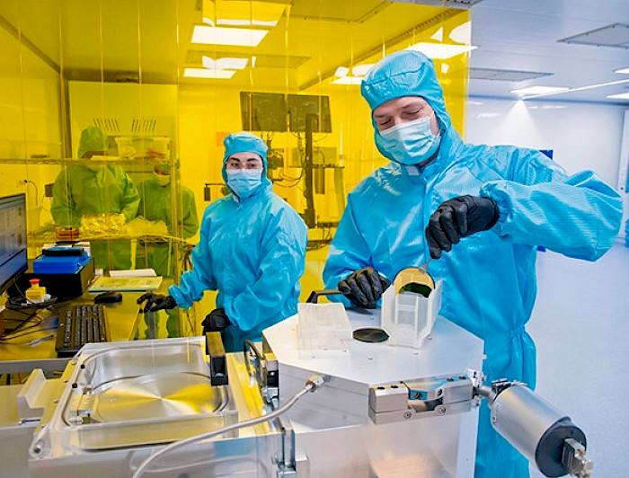
photo_camera This is the largest cleanroom in Chile and the first in the region to be designed for teaching. (Photo credit: Faculty of Physics)
Cleanrooms are key spaces for material physics research.
They are designed to reduce contamination and the control of different variables, such as environmental humidity, temperature, atmospheric pressure, and static, is crucial.
The achievement of the Faculty of Physics of UC Chile is so valuable for that very reason. On its 40th anniversary, the Faculty of Physics inaugurated the Functional Materials & Devices Lab —AKA the largest cleanroom in Chile and the first in South America to have been originally designed for teaching and learning.
"Implementing and operating a cleanroom is a major challenge, so it took us many years to raise the resources to execute the project. Today, we have the largest cleanroom in Chile, 127 square meters in total, 90 of which have filtered air, with very low levels of contamination, which allows us to do research in a very efficient way", explained Loïk Gence, researcher at the UC Chile Institute of Physics and one of the leaders of the project.
"The big difference with other cleanrooms in South America is that ours was designed from the outset as a multidisciplinary project, allowing free access for research, collaboration, and teaching."
Impact on Students
Since the cleanroom is open to students, it gives them a great opportunity to be introduced to the world of research and experimental physics.
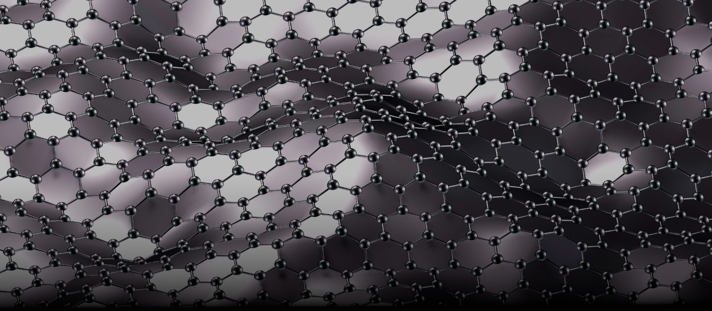
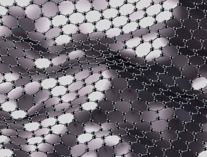
As a matter of fact, more than 50 undergraduate and graduate students in Physics, Engineering, and Chemistry have learned to use it so far. They have made lithographs and have manufactured complete graphene-based devices. This fantastic material, which comes from graphite, is the result of the dense clustering of carbon particles in hexagonal sheets and is known as the material of the future.
"Working with graphene is very interesting for students because it is a very new, versatile and functional material with extraordinary properties: it has very good electrical conductivity, is transparent, flexible, and has excellent mechanical strength. All these properties allow it to be used for the fabrication of transistors and advanced devices, such as photodetectors, solar cells, or electrical inverters, which is what our students worked with. While this type of device exists in the industry, our students learned to make it from scratch. To do so, they understood the physical basis of graphene, manipulated it, and created a key element for electronic devices," explained Loïk Gence.
A Cleanroom with State-of-the-Art Equipment
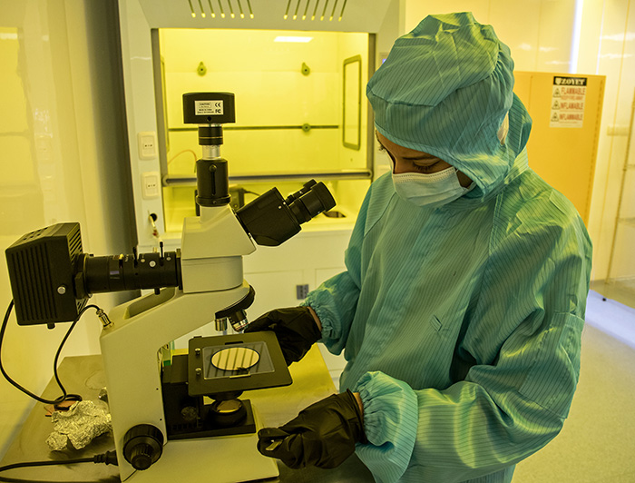
While its cleanliness makes it unique, it is not the only interesting thing about the room; its equipment is also notable.
In fact, Loïk Gence, a faculty member from the Faculty of Physics, and Roberto Rodríguez, director of the Institute of Physics, were recently awarded funds for the acquisition of highly specialized equipment. These make it possible to work with any material, structure it, and modify it to make technological applications.
The first batch of equipment is already installed and operational, and facilitates micro-manufacturing, something relatively new in Chile. In a special built-in chamber, the equipment generates plasma capable of controlling matter and removing it at a nanometer scale.
This allows for high-quality optical work, for example. This type of optics requires working with clean lenses and perfect geometry. The lenses are made of a glass on which a very thin layer of aluminum or other reflective metal is deposited. That metal must be uniform, consistent, flawless, and clean.
The equipment in the cleanroom makes it possible to create such lenses, as it is possible to manipulate the thin layers and adjust their thickness at a nanometer level. If there are defects in the mirror, the metal layer can be removed and repaired without damaging the lens.
The second piece of equipment—to be installed in the coming months—will be used to add materials to a surface.
With a technique called sputtering, the machine generates a mini plasma that vaporizes metals, making alloys between them. The metals can be combined according to their properties (as electrical insulators, semiconductors or superconductors) and then deposited on glass to produce a mirror.
"This equipment will give our undergraduate students access to tools that are available at the best universities in the world, and they will be able to develop top-notch devices," explained researcher Gence.
Learn more about the work being done at the Functional Materials & Devices Lab.


